


Báo cáo hóa học: " Fabrication of ordered nanoporous anodic alumina prepatterned by mold-assisted chemical etching"
lượt xem 9
download
 Download
Vui lòng tải xuống để xem tài liệu đầy đủ
Download
Vui lòng tải xuống để xem tài liệu đầy đủ
Tuyển tập báo cáo các nghiên cứu khoa học quốc tế ngành hóa học dành cho các bạn yêu hóa học tham khảo đề tài: Fabrication of ordered nanoporous anodic alumina prepatterned by mold-assisted chemical etching
Bình luận(0) Đăng nhập để gửi bình luận!
Nội dung Text: Báo cáo hóa học: " Fabrication of ordered nanoporous anodic alumina prepatterned by mold-assisted chemical etching"
- Lai et al. Nanoscale Research Letters 2011, 6:157 http://www.nanoscalereslett.com/content/6/1/157 NANO EXPRESS Open Access Fabrication of ordered nanoporous anodic alumina prepatterned by mold-assisted chemical etching Kuan-Liang Lai1, Min-Hsiung Hon1, Ing-Chi Leu2* Abstract In this article, a simple and cost-effective method to create patterned nanoindentations on Al surface via mold- assisted chemical etching process is demonstrated. This report shows the reaction-diffusion method which formed nanoscale shallow etch pits by the absorption/liberation behaviors of chemical etchant in poly(dimethylsiloxane) stamp. During subsequent anodization, it was possible to obtain the ordered nanopore arrays with 277 nm pitch that were guided by the prepatterned etch pits. The prepatterned etch pits obtained can guide the growth of AAO nanopores during anodization and facilitate the preparation of ordered nanopore arrays. Introduction anodization [8-10]. Despite the ideally ordered patterns In recent years, nanoporous anodic aluminum oxide obtained, this method is limited by the pattern transfer (AAO) has become a popular template system for the protocol, and pattern transferred by imprint lithography synthesis of various functional nanostructures which directly onto metallic substrates such as Al foils or Al have extensive applications in scientific and commercial films requires 50-2000 times higher pressures in com- fields [1-4]. In the syntheis of template-based materials, parison with imprint lithography on polymer layers [11]. the template with long-range-ordered nanostructure is The applied pressure for pattern transfer tends to crack attractive, in order that structurally well-defined materi- the substrates underneath the Al films, such as silicon als can be consequently produced. In general, Al anodi- and glass with brittle property, and leads to substrate zation processes, highly regular arrangement of pores, fracture. Otherwise, damage to the imprint stamp often however, occurs only within a small process window, occurs after several runs of imprinting because of the and the domain size (ordering length) is usually limited high mechanical stresses. to a micrometer scale on Al foils [5,6]. In order to In the reported literatures, some outstanding methods, achieve an ordered pore arrangement over a larger area, such as focused ion beams [6], optical diffraction grat- Masuda et al. [5,7] developed a pretexturing process of ings [12], colloidal lithography [13], block-copolymer Al using nanoimprinting with a SiC mold. Shallow self-assembly [14], and metal mask [15] were also used indentations on an Al substrate initiate pore nucleation to achieve prepatterning of Al substrates, thus avoiding during anodization and lead to a long-range-ordered fabrication of the expensive hard imprint stamp. How- pore arrangement within the stamped area. ever most of them have limitations in scalability or size Self-ordered and prepatterned guided growths are two of ordered domains. Consequently, a simple and eco- kinds of anodization technology, which are competing nomic method for realization of a long-range-ordered AAO over very large areas (cm2 to wafer size) still faces in the aspects of product quality and production cost. For prepatterned guided anodization, imprinting meth- challenges. Recently, some methods, such as guided ods have been used by several author groups to prepare electric field method [16], and step and flash imprint ordered AAO, wherein nanoindentations are created by lithography [17], have been developed to fabricate transferring patterns from hard master stamp onto the wafer-scale-ordered AAO. Al surface under a high pressure (5-25 kN cm-2) before Ideally, a simple and cost-effective process for preparing ordered AAO should combine with a high- throughput method to create patterned nanoindenta- * Correspondence: icleu@mail.mse.ncku.edu.tw 2 Department of Materials Science, National University of Tainan, Tainan 700, tions on Al surface. It should also be substrate-friendly Taiwan. Full list of author information is available at the end of the article © 2011 Lai et al; licensee Springer. This is an Open Access article distributed under the terms of the Creative Commons Attribution License (http://creativecommons.org/licenses/by/2.0), which permits unrestricted use, distribution, and reproduction in any medium, provided the original work is properly cited.
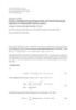
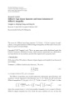
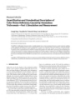
- Lai et al. Nanoscale Research Letters 2011, 6:157 Page 2 of 6 http://www.nanoscalereslett.com/content/6/1/157 anodization was conducted under a constant voltage in to avoid damaging the substrate such as thin Al film- phosphoric acid solution. The ordered AAO structures deposited Si. were examined by scanning electron microscopy (SEM, The reaction-diffusion wet stamping (RD-WETS) Hitachi S3000) and atomic-force microscopy (AFM, method uses a nanopatterned agarose stamp such as Digital Instrument Nanoscope LFM-3). poly(dimethylsiloxane) (PDMS) in soft lithography. An agarose stamp soaked with an appropriate chemical Results and discussions reactant can etch/dissolve the desired hard material by simply contacting with the substrate (e.g., HF for SiO2 The RD-WETS approach can be extended to structuring or HCl/FeCl 3 for Cu) [18-20]. Localized etching is hard materials by chemical etching reaction. Regardless mediated by a mold-assisted chemical etching initiated of the substrate type, the mechanism of localized micro- from the stamp microfeatures, and excellent uniformity etching relied on the diffusive transport of chemicals over areas of several square centimeters can be achieved. within a stamp [18-20]. Figure 1 shows the scheme of In this study, a simple and reliable method for sub- mold-assisted microetching of substrate. The PDMS strate prepatterning by soft imprinting, using a diffu- stamp was soaked in etching solution (2% mixed acid in sion-reaction-controlled wet chemical etching method, alcohol) for 10 min and absorbed approximately 4% is developed thus avoiding the use of sophisticated etching solution, and the residual solution on the sur- device fabrication procedures. In addition, the highly face of stamp was removed by N2 flow. Then, the wet ordered porous alumina on Al foils with the help of pre- stamp was set on Al substrate with a slight loading patterned indentations by the above-mentioned wet (0.01 MPa) to ensure a conformal contact with sub- stamping were fabricated. strate. The etchant-contained alcohol liberated from stamp reacted with Al metal, and the reaction products Experimental section diffused into PDMS along the concentration gradient as the arrows indicated. Compared with the conventional The master molds for PDMS stamp fabrication were RD-WETS process, this method used alcohol in place of sub-micromter gratings (for 1D pattern) and Si wafers water because the alcohol in agarose mold has a higher with regular pit arrays (for 2D pattern). The membrane absorptivity than water [21]. It helps to adjust the stamp was made by pouring a mixture of PDMS prepo- degree of reaction-diffusion by the solvent liberation/ lymer (Dow Corning Sylgard 184) and its curing agent absorption process and this two-way chemical “pump” (10:1 by weight) into the masters, which was cured for increases the work efficiency. From this point of view, 1 h at room temperature and then for 4 h at 60°C in an the parameters of RD process should be adjusted to oven. The PDMS stamps about 2 mm in thickness were meet the requirements of imprinting nanopatterns on replicated from straight line diffraction grating surface Al surface. In general, the shallow nanoscale concave (Thorlabs, Inc. 3600 and 1800 lines/mm), and Si mold (just 3 nm in depth is sufficient) can guide the ordered with regular pit arrays of 277-nm pitch. The flexible growth of AAO effectively [9]. agarose membrane has a better attachment to solid sur- face. Al samples with a total surface area of 2 × 2 cm2 The photograph of sample after RD-WETS is shown in Figure 2a, where the Al surface with grating prepat- were cut from an aluminum sheet (99.99%, Alfa Aesar), tern appears under visible diffractive light and results in degreased in acetone and dried. a uniform prepattern over large areas (up to 2 × 2 cm2). The Al sheet was electropolished at a constant voltage in perchloric acid/ethanol (1:4 V/V ratio) at 4°C for A detailed investigation of the film topography was per- 30 s, to diminish the roughness of Al foil surface. Pat- formed by AFM as Figure 2b,c shows. The pitches of terns on Al substrate were etched using a mold pre- grating patterns are 555 and 277 nm with pattern viously soaked in a diluted solution of mixed acid (2%) heights of 40 and 25 nm, respectively. Overall, the reac- in alcohol (mixed acid composition: 0.15 M HNO 3 , tion-diffusion process allowed the PDMS to cut into the Al substrate, in particular, with retention of the stamp’s 0.6 M H3PO4, and 0.2 M CH3COOH). The nitric acid topography. consumes some of the aluminum material to form an After the RD process, anodization was conducted aluminum oxide layer. This oxide layer is then dissolved under a constant voltage of 110 V in 0.3 M H 3PO4 at by the phosphoric acid, and more Al 2O3 is formed to keep the oxidation/dissolution cycle going. The diluted 5°C. The anodization voltage for the prepatterned alumi- etchants moderated the condition of etching reaction num substrate was chosen to satisfy the linear relation- and contributed to the formation of nanopatterns. The ship between the interpore distance and the anodization potential (2.5 nm/V-1) reported for the common anodi- PDMS stamp was soaked in etching solution for 10 min and absorbed in the latter, and the time period for etch- zation process [22]. Figure 3 shows SEM micrographs of ing process was within 5 min. After nanoindentation by alumina pores obtained from aluminum foils, half of the RD-WETS process with PDMS membrane stamps, which (left-hand side) were obtained on Al pretextured
- Lai et al. Nanoscale Research Letters 2011, 6:157 Page 3 of 6 http://www.nanoscalereslett.com/content/6/1/157 Etching solution liberated Wet PDMS mold Al metal Localized etching (two-way chemical ‘pump‘ ) Figure 1 Scheme of the experimental procedures for reaction-diffusion wet etching. The results shown in Figure 4b confirm that the predeter- by RD-WETS. Pores arranged in a 1D grating configura- mined pattern can act as initiation points and guide the tion were observed only in the pretextured area, while growth of channels in the oxide film. Straight oxide nano- the disordered pores were found in the untreated area. channels (Figure 4c) with uniform-sized pores are obtained. In addition, it was found that the PDMS stamp can well Furthermore, the two-step imprinting was used to fab- tolerate the dilute acid etchant, which implies that the ricate multiple patterns from a single master. The two- soft stamp can be reused multiple times without notice- step imprinting can be used to selectively etch Al at able decrease in patterning quality [18]. established primary structure because the etchant only Furthermore, the 2D periodic prepattern on Al was fabri- acts at the contact site between the mold and substrate cated using a PDMS mold with square dot arrays, as Figure [18]. After the first mold-assisted etching, a second etch- 4a shows. Shallow etched pits in the prepattern (approxi- ing step was performed using the same grating rotated mately 40-nm depth) serves as nucleation sites for the by approximately 85° around the axis perpendicular to development of a pore in the early stage of anodization the surface to discriminate this multiple case from one- [5-7], and results in the eventual growth of a pore channel. a b 40nm c 25 nm Figure 2 The photograph and AFM images of the aluminum substrate with grating prepatterns (a) sample after RD-WETS . (b) procedure with pitch of 555 nm; (c) 277 nm.
- Lai et al. Nanoscale Research Letters 2011, 6:157 Page 4 of 6 http://www.nanoscalereslett.com/content/6/1/157 a 10 m b c 5m 5m Figure 3 SEM micrographs of anodization sample (a) alumina pores obtained from aluminum foils. (b) alumina pores grown in the 1D grating-patterned area. (c) alumina pores grown in the unpatterned area. Anodization conducted in 0.3 M H3PO4 at 110 V and 5°C. a 40nm c b 2m 100 nm Figure 4 AFM and SEM images of Al prepattern and AAO (a) 2D Al prepatten after RD-WETS. (b, c) 2D prepattern-induced regular AAO array. Anodization conducted in 0.3 M H3PO4 at 110 V and 5°C.
- Lai et al. Nanoscale Research Letters 2011, 6:157 Page 5 of 6 http://www.nanoscalereslett.com/content/6/1/157 aim of fabricating nanostructured functional AAO with s tep imprinting method. A parallelogram profile of required design geometry. etched pit arrays was obtained, as illustrated in Figure 5a,b. From the AFM images, the intersects of grating Conclusions pattern show shallow indent arrays which resemble point-like depressions [5,12] and have just several nan- In conclusion, a novel method for fabricating prepatterned ometers in depth relative to the local surface around Al foil was developed, which used the reaction-diffusion them. In addition, the double-etching sites serve as the process mediated by a PDMS template. By means of using nucleation sites, and the ordered AAO growth can be the diluted (2%) mixed acid solution as a chemical etchant, maintained as shown in Figure 5c,d. A single pore just the wet soft stamp can indent nanoscale shallow concaves appears on double-etching site and the notches of multi- on aluminum without the need of excessive loading. ple etching remain on the AAO surface and parallelo- Furthermore, based on the phenomenon of multiple RD- gram (i.e., non-right angle) patterns of pore arrays are WETS imprinting, 2D prepattern by multiple etching obviously different from the directly imprinted 2D could be made using simple stripe-patterned stamps with square prepatterns (Figure 4b). All of these experimental selected orientation. After anodization, a uniform, ordered findings suggest that this mold-assisted etching method AAO array with 277-nm interpore distance guided by the is industrially applicable to a large-scale production of prepattern was obtained. Combining mold-assisted chemi- nanopatterning and has the potential of achieving the cal etching and anodization reaction, this process provides 1st 2nd b a Initiation site c d 1m 5m Figure 5 AFM and SEM images of Al prepattern and AAO (a, b) Al prepattern featuring a second grating on a primary structure with ~85° rotation and pitch of 277 nm. (c, d) prepattern-induced regular AAO array. Anodization conducted in 0.3 M H3PO4 at 110 V and 5°C.
- Lai et al. Nanoscale Research Letters 2011, 6:157 Page 6 of 6 http://www.nanoscalereslett.com/content/6/1/157 a simple and efficient route to obtain ordered nanostruc- 14. Kim B, Park S, McCarthy TJ, Russell TP: Fabrication of Ordered Anodic Aluminum Oxide Using a Solvent-Induced Array of Block-Copolymer tures for further nanodevice applications. Micelles. Small 2007, 3:1869. 15. Zhao X, Jiang P, Xie S, Feng J, Gao Y, Wang J, Liu D, Song L, Liu L, Dou X, Luo X, Zhang Z, Xiang Y, Zhou W, Wang F: Patterned anodic aluminium Abbreviations oxide fabricated with a Ta mask. Nanotechnology 2006, 17:35. AAO: anodic aluminum oxide; PDMS: poly(dimethylsiloxane); RD-WETS: 16. Nasir ME, Allsopp DWE, Bowen CR, Hubbard G, Parsons KP: The fabrication reaction-diffusion wet stamping. of mono-domain highly ordered nanoporous alumina on a wafer scale by a guided electric field. Nanotechnology 2010, 21:105303. Acknowledgements 17. Kustandi TS, Loh WW, Gao H, Low HY: Wafer-scale near-perfect ordered The financial support of this study from the National Science Council, porous alumina on substrates by step and flash imprint lithography. ACS Taiwan ROC (NSC 97-2628-E-006-122 and NSC 99-2221-E-024-004) is Nano 2010, 5:2561. gratefully appreciated. 18. Grzybowski BA, Bishop KJM: Micro- and nanoprinting into solids using reaction-diffusion etching and hydrogel stamps. Small 2009, 5:22. Author details 19. Grzybowski BA, Bishop KJM, Campbell CJ, Fialkowski M, Smoukov SK: Micro- 1 Department of Materials Science and Engineering, National Cheng Kung and nanotechnology via reaction-diffusion. Soft Matter 2005, 1:114. University, Tainan 701, Taiwan. 2Department of Materials Science, National 20. Smoukov SK, Grzybowski BA: Maskless Microetching of Transparent University of Tainan, Tainan 700, Taiwan. Conductive Oxides (ITO and ZnO) and Semiconductors (GaAs) Based on Reaction-Diffusion. Chem Mater 2006, 18:4722. Authors’ contributions 21. Lee JN, Park C, Whitesides GM: Solvent Compatibility of Poly MHH and ICL planned and supervised the research project. ICL, KLL and (Dimethylsiloxane)-Based Microfluidic Devices. Anal Chem 2003, 75:6544. MHH conceived and designed the experiments. KLL carried out the 22. Ono S, Masuko N: Evaluation of pore diameter of anodic porous films experiments, analyzed the data, and drafted the manuscript. ICL participated formed on aluminum. Surf Coat Technol 2003, 169:139. in the analysis of experimental data and the writing of manuscript. All authors discussed the results and commented on the manuscript. doi:10.1186/1556-276X-6-157 Cite this article as: Lai et al.: Fabrication of ordered nanoporous anodic alumina prepatterned by mold-assisted chemical etching. Nanoscale Competing interests Research Letters 2011 6:157. The authors declare that they have no competing interests. Received: 2 October 2010 Accepted: 21 February 2011 Published: 21 February 2011 References 1. Lee W, Scholz R, Nielsch K, Gosele U: A Template-Based Electrochemical Method for the Synthesis of Multisegmented Metallic Nanotubes. Angew Chem Int Edn 2005, 44:6050. 2. Park S, Lim JH, Chung SW, Mirkin CA: Self-assembly of mesoscopic metal- polymer amphiphiles. Science 2004, 303:348. 3. Zhi L, Wu J, Li J, Kolb U, Mullen K: Carbonization of Disc-like Molecules in Porous Alumina Membranes: Toward Carbon Nanotubes with Controlled Graphene Layer Orientation. Angew Chem Int Edn 2005, 44:2120. 4. Wang Z, Brust M: Fabrication of nanostructure via self-assembly of nanowires within the AAO template. Nano Res Lett 2007, 2:34. 5. Masuda H, Yamada H, Satoh M, Asoh H, Nakao M, Tamamura T: Highly Ordered Nanochannel-Array Architecture in Anodic Alumina. Appl Phys Lett 1997, 71:2770. 6. Liu CY, Datta A, Wang YL: Ordered Anodic Alumina Nanochannels on Focused-Ion-Beam-Prepatterned Aluminum Surfaces. Appl Phys Lett 2001, 78:120. 7. Asoh H, Nishio K, Nakao M, Tamamura T, Masuda J: Conditions for fabrication of ideally ordered anodic porous alumina using pretextured Al. J Electrochem Soc 2001, 148:B152. 8. Choi JS, Sauer G, Goring P, Nielsch K, Wehrspohn RB, Gosele U: Monodisperse metal nanowire arrays on Si by integration of template synthesis with silicon technology. J Mater Chem 2003, 13:1100. 9. Yasui K, Nishio K, Nunokawa H, Masuda H: Ideally ordered anodic porous alumina with sub-50 nm hole intervals based on imprinting using metal molds. J Vac Sci Technol B 2005, 23:L9. Submit your manuscript to a 10. Lee W, Ji R, Ross CA, Gosele U, Nielsch K: Wafer-scale nickel imprint stamps for porous alumina membranes based on interference journal and benefit from: lithography. Small 2006, 2:978. 11. Chou SY, Krauss PR, Renstrom PJ: Imprint of sub-25 nm vias and trenches 7 Convenient online submission in polymers. Appl Phys Lett 1995, 67:3114. 7 Rigorous peer review 12. Mikulskas I, Juodkazis S, Tomasiumas R, Dumas JG: Aluminium oxide 7 Immediate publication on acceptance photonic crystals grown by a new hybrid method. Adv Mater 2001, 13:1574. 7 Open access: articles freely available online 13. Fournier-Bidoz S, Kitaev V, Routkevitch D, Manners I, Ozin GA: Highly 7 High visibility within the field ordered nanosphere imprinted nanochannel alumina (NINA). Adv Mater 7 Retaining the copyright to your article 2004, 16:2193. Submit your next manuscript at 7 springeropen.com
CÓ THỂ BẠN MUỐN DOWNLOAD

-

Báo cáo hóa học: "Research Article Detecting and Georegistering Moving Ground Targets in Airborne QuickSAR via Keystoning and Multiple-Phase Center Interferometry"
 11 p |
  116
|
116
|  7
7
-
Báo cáo hóa học: "Research Article Are the Wavelet Transforms the Best Filter Banks for Image Compression?"
7 p | 120
| 7
-

Báo cáo hóa học: " Research Article Practical Quantize-and-Forward Schemes for the Frequency Division Relay Channel"
11 p | 114
| 6
-
Báo cáo hóa học: " Research Article Breaking the BOWS Watermarking System: Key Guessing and Sensitivity Attacks"
8 p | 104
| 6
-
Báo cáo hóa học: " Research Article A Fuzzy Color-Based Approach for Understanding Animated Movies Content in the Indexing Task"
17 p | 108
| 6
-
Báo cáo hóa học: "Research Article Cued Speech Gesture Recognition: A First Prototype Based on Early Reduction"
19 p | 116
| 6
-

báo cáo hóa học:" Recombinant bromelain production in Escherichia coli: Process optimization in shake flask culture by Response Surface Methodology"
34 p | 96
| 6
-
Báo cáo hóa học: "Research Article Color-Based Image Retrieval Using Perceptually Modified Hausdorff Distance"
10 p | 97
| 5
-

Báo cáo hóa học: " Yeast expressed recombinant Hemagglutinin protein of Novel H1N1 elicits neutralising antibodies in rabbits and mice"
29 p | 76
| 5
-

Báo cáo hóa học: " Research Article Some Geometric Properties of Sequence Spaces Involving Lacunary Sequence"
8 p | 94
| 5
-
Báo cáo hóa học: "Research Article Exploring Landmark Placement Strategies for Topology-Based Localization in Wireless Sensor Networks"
12 p | 118
| 5
-
Báo cáo hóa học: " Research Article A Motion-Adaptive Deinterlacer via Hybrid Motion Detection and Edge-Pattern Recognition"
10 p | 93
| 5
-
Báo cáo hóa học: "Research Article Probabilistic Global Motion Estimation Based on Laplacian Two-Bit Plane Matching for Fast Digital Image Stabilization"
10 p | 112
| 4
-

báo cáo hóa học:" Sparse correlation matching-based spectrum sensing for open spectrum communications"
43 p | 74
| 4
-
Báo cáo hóa học: "Research Article On the Generalized Favard-Kantorovich and Favard-Durrmeyer Operators in Exponential Function Spaces"
12 p | 102
| 4
-
Báo cáo hóa học: " Research Article Hilbert’s Type Linear Operator and Some Extensions of Hilbert’s Inequality"
10 p | 77
| 4
-
Báo cáo hóa học: "Research Article Quantification and Standardized Description of Color Vision Deficiency Caused by"
9 p | 120
| 4
-

Báo cáo hóa học: " Cytopathic Mechanisms of HIV-1"
22 p | 78
| 4


Chịu trách nhiệm nội dung:
Nguyễn Công Hà - Giám đốc Công ty TNHH TÀI LIỆU TRỰC TUYẾN VI NA
LIÊN HỆ
Địa chỉ: P402, 54A Nơ Trang Long, Phường 14, Q.Bình Thạnh, TP.HCM
Hotline: 093 303 0098
Email: support@tailieu.vn
Giấy phép Mạng Xã Hội số: 670/GP-BTTTT cấp ngày 30/11/2015 Copyright © 2022-2032 TaiLieu.VN. All rights reserved.

